Here's a review of free Linux Gerber file viewers.
PCB fabrication shops usually require Gerber files of your latest PCB design. Taking one last look can prevent mistakes, so you'll want to view the designs graphically with a Gerber file viewer.
Windows users have quite a few options which I've previously reviewed. For Linux users the choices are very limited but here's my review of the available options.
Showing posts with label tools. Show all posts
Showing posts with label tools. Show all posts
Wednesday, October 23, 2013
Friday, October 28, 2011
Measuring Motor Current
I need to measure the current going through brushed DC motors. One of the ways to do this is to use a shunt resistor, a low-value, precision resistor. Measuring the voltage drop across the resistor, one can calculate the current through the resistor.

I decided to make my very own, very simple, shunt resistor breakout board. It connects between the battery and Electronic Speed Controller (ESC) or other motor driver.

A header is included to measure voltage across the battery and voltage drop across the resistor either with a DMM or a microcontroller.
 |
| DMM test clips attached |
I quickly drew up the design in Eagle, used toner transfer method and etched the board, soldered everything together and voila, simple current measurement.
 |
| Pretty simple circuit board, eh? |
 |
| 0.001 ohm, 1%, 3W = 50A+ (WSR31L000FEA) |
The resistor is 0.001 ohms so 1mV = 1A (it's a Dale-Vishay WSR31L000FEA). My DMM has precision to 0.1mV, thus 100mA here. I selected a resistor with sufficient power handling to measure over 50A continuously.
So what the heck am I going to do with this thing?
- Measure RC airplane propeller load on motor
- Calculate battery internal resistance
- Plot relationship between motor current and compass distortion
- Calculate remaining battery capacity on an autonomous robot
- Overcurrent protection
- Create a digital ammeter with an MCU and LCD display
Some add-on hardware is needed to interface with a microcontroller. The AttoPilot shunt boards use a Texas Instruments INA-169 for amplifying voltage drop across the shunt to a suitable range for an analog to digital converter. (While I am using the simpler board above for bench testing, I decided to get the AttoPilot board for use on Data Bus)
One has to be careful, of course, that the shunt presents substantially less resistance than the load. Some motors have very low resistance windings. For those cases, a hall effect sensor like the Honeywell CSLA2CD seems like it would do the trick.
 |
| AttoPilot current/voltage sense board |
Friday, September 2, 2011
A Review of Free Windows Gerber File Viewers
When you send off your latest PCB design to a PCB fabrication shop you'll typically send Gerber files. You probably want to perform a final proof-read of your design, so you'll need a Gerber file viewer to view your files graphically. If you're cheap like me you want a free Gerber viewer. Here's a brief review of truly free Gerber file viewers for Windows.
Tuesday, June 21, 2011
Tools: Equation Editor (take 2)
[let's try this again...*ahem*]
A couple months ago I found this neato equation editor/creator that generates a nice equation image. Handy for us technical bloggers. I've already used it on several posts. Enjoy!
http://www.codecogs.com/latex/eqneditor.php
Sorry about the mishap yesterday.
A couple months ago I found this neato equation editor/creator that generates a nice equation image. Handy for us technical bloggers. I've already used it on several posts. Enjoy!
http://www.codecogs.com/latex/eqneditor.php
Sorry about the mishap yesterday.
Friday, May 6, 2011
101 Tools for the Roboticist
A recent issue of Robot Magazine included a nicely done writeup on the merits of Oscilloscopes for robotics hobbyists. I totally agree.
The article got me to thinking about the tools I use. Not the obvious ones like Digital Multimeters or the cool ones like Bus Pirates or Logic Analyzers, but the tools that are indispensable yet are never the first to come to mind. They're the unsexy underdogs of the robotics hobby world...
001. Paper and writing utensil: Even after almost 2000 years, the convenience and immediacy of paper has yet to be surpassed. Having a big stash of scrap, blank paper and pencils/pens is awfully handy for capturing thoughts, doing calculations, drawing designs, drawing robots, and the like. The key is having a stash you can grab from lickety split.
010. Laser Printer: I've used it to create PCB transfers, test PCB sizing, make hardcopies of various robotics and electronics information for quick reference, and generate templates for drilling/cutting robot chassis, among many other things. My old Laserjet 4m+ is an industrial strength workhorse and should last another 20 years without any trouble.
011. LEDs: Cheap, simple diagnostic tool, like an in-circuit logic probe. Throw one on the protoboard to make sure the power's on. Throw one on a line that's supposed to be high. Throw another on the motor when it's on or use dual color to show direction.
100. Cordless Drill: Great for driving screws for assembly/disassembly, drilling holes, chamfering or countersinking, can also use for twisting wires together (put one end in the vise, chuck the other end, and begin).
101. Flux: Even with the best iron, solder work/rework is going to be poor without flux, which allows molten solder to flow better. I'd rather have flux than a good iron. The best choice is a flux pen like ones from Kester, but Radio Shack flux paste, while messy, works and is good at sticking SMD parts onto PCBs.
Saturday, January 23, 2010
ESR Test Harness: Part 2
Version 2
 You may recall the original article on the Equivalent Series Resistance test harness. Well, it's been several weeks since I looked at this project and I wanted to finish it. I have a lot of capacitors to test!
Upon revisiting, I figured it best to prototype the more complex circuit from Stephen M. Powell's website before proceeding further.

Upon revisiting, I figured it best to prototype the more complex circuit from Stephen M. Powell's website before proceeding further.
After working out the kinks, I reworked the original schematic and board layout and selected a larger enclosure primarily to make more room for front panel knobs and switches. So it ended up being something of a do-over.
Over the course of a few days I built up the ESR test harness, worked out a few glitches, and now have a useful, attractive, working test tool for the bench. Here's how. (And how not)
Lessons Learned
Here's the circuit I built from, most of it verified by prototyping and testing. For details on how the circuit works you can reference Powell's test harness article. This article focuses more on prototyping, testing, building -- and screwing up -- in hopes it will help you.

Over Voltage Diode Problems
I started with a simpler version of the circuit for prototyping, leaving out the over-voltage protection diodes and potentiometers. The circuit produced a nice 80kHz square wave.
Adding the over-voltage protection diodes created some funky ramp waveforms as if the P-N junctions were conducting--they shouldn't have been--so I fiddled with resistor R3 to drop the amplitude well below 0.6V and then the 'scope displayed a nice, happy square wave.
Screwing Up Resistors
What I didn't know at the time was that the resistors I thought were 22Ω were actually 220Ω (the brown band looked black to me). So R4 and R5/R6 dropped too much voltage, activating the diodes.
Additionally, the circuit didn't do a good job measuring ESR after I'd finished building the final product. Powell's original choice of R3 and R4 work best and once I'd replaced R3 (470Ω), R4 (22Ω) and R5/R6 (just one 6.8Ω resistor I had on hand worked as well as Powell's 10Ω) , I got the result I wanted... well, almost.
For this and several other reasons, prototyping and testing the complete circuit before fabricating is crucial. I did that, but fixed the wrong thing, tested wrong, and tested the wrong thing.
Variable Frequency, Duty Cycle
For adjustable frequency, I added in the 1MΩ potentiometer to the prototype and found I had to add a 1.8Ω resistor in series to ensure a minimum resistance. Without that minimum resistance, the waveform went funky at the potentiometer's lower extreme. Good thing I tested. Of course, you can always wire resistors in point-to-point to fix stuff if necessary. With the series resistor, frequency is indeed variable from about 1kHz to 300kHz. Cool.
Duty cycle can be changed and I built that capability into the PCB but set it at a fixed value as it wasn't all that useful.
Screwing up the Schematic
Then I discovered a pretty big error in my schematic. The 555 square wave circuit I'd drafted was very different from Powell's. Glad I caught that before I made the PCB because that would've been a serious pain in the rear.

Screwing Up Testing
In addition to using the wrong resistors, my oscilloscope probe was set to 10X (attenuating the signal by 10). After fixing the resistors and the probe, the circuit had good sensitivity to low ESR.
Quick Translation Table
How do you translate screen reading to ESR? I put together a table and graph to translate directly from waveform amplitude in 'scope divisions to ESR value.
Measuring amplitude out of pin 3 on the 555, and then calculating total resistance and thus current, it was possible to calculate voltage drop for various ESR capacitors in parallel with R5 (6.8Ω), then convert that to the number of divisions on the scope, when it's set to either 5mV/division or 10mV/divison.

 The graph makes it easy to quickly read ESR based on amplitude of the waveform across a test capacitor. With the scope set to 10mV/division, here are the heuristics restated:
PCB Fabrication Tips
As before, I put together the schematic and board layout in Eagle. This time I used copper pour regions (polygons in Eagle) for ground so that less etching, and etchant, were necessary.

I found that soldering components to the big swaths of copper is tricky so next time I will try using "thermals" which adds some space around the pads to ensure most of the heat is directed at the pad (see below)
 Thermal pad isolation, detail
Screwing Up PCB Fabrication
As with my prior attempts at DIY PCB etching, I found the method using magazine paper and clothes iron transfer is still a bit tough to get right. The magazine paper kept jamming in the laser printer. Also, it's important to let the transfer and board cool down before messing with it, otherwise you'll peel the magazine paper away and ruin the transfer. When ironing, the length of time and amount of pressure remains important. Too much pressure and time and the traces get blotchy. Too little time and the transfer isn't thorough. After a couple outright failures, I got a transfer that was good enough, but certainly not great.


PCB after transfer (left) and after etching (right)
The etching method using Ferric Chloride with a sponge still takes forever. Frankly for all that scrubbing, I'd just as soon dump the board in a tank and let it sit for an hour (or however long it takes). Plus there would be less risk of spilling FeCl all over the garage floor (yes, my garage floor now has giant yellow spots), my clothes, hands, etc. I'll try that approach next time.
Drilling
Drilling went ok. I used the drill map approach from last time wherein my Perl script converts a drill file into a CSV that can be imported and graphed in Excel or OpenOffice Calc. I again used a scatter plot in OpenOffice Calc to draw a diagram showing what drill sizes to use for each hole.
 Board Assembly
Most of the components I had on hand. For testing, I used bus wire to jumper out the variable resistors and a simple 9V connector for power. When I powered it up and connected to the scope, it displayed a waveform. As described above I had to fix some glitches to get it working right.


The finished board (left) works (right)
Screwing Up Some More
The main probe BNC, on the schematic, wires in series with a 22kΩ resistor. I think it's another overvoltage protection feature. After building everything I discovered this resistor messes up the square wave sent to the scope and jacks up the signal at higher frequencies. I never caught this because I never tested this aspect of the circuit properly.

Meanwhile, the waveform across the 6.8Ω resistor looks good (though with some ringing). A couple options exist.
Over the course of a few days I built up the ESR test harness, worked out a few glitches, and now have a useful, attractive, working test tool for the bench. Here's how. (And how not)
Lessons Learned
- Prototype, use and test the entire circuit as designed before fabricating a PCB
- Check the schematic for correctness carefully before fabricating the PCB
- Use copper pour regions where possible so there's less copper to etch away
- Try using thermals for pads on copper pour regions to improve soldering
- When selecting the enclosure consider: availability, interface design and size, circuit size, and power supply size.
- Don't be an idiot like me...
Here's the circuit I built from, most of it verified by prototyping and testing. For details on how the circuit works you can reference Powell's test harness article. This article focuses more on prototyping, testing, building -- and screwing up -- in hopes it will help you.

Over Voltage Diode Problems
I started with a simpler version of the circuit for prototyping, leaving out the over-voltage protection diodes and potentiometers. The circuit produced a nice 80kHz square wave.
Adding the over-voltage protection diodes created some funky ramp waveforms as if the P-N junctions were conducting--they shouldn't have been--so I fiddled with resistor R3 to drop the amplitude well below 0.6V and then the 'scope displayed a nice, happy square wave.
Screwing Up Resistors
What I didn't know at the time was that the resistors I thought were 22Ω were actually 220Ω (the brown band looked black to me). So R4 and R5/R6 dropped too much voltage, activating the diodes.
Additionally, the circuit didn't do a good job measuring ESR after I'd finished building the final product. Powell's original choice of R3 and R4 work best and once I'd replaced R3 (470Ω), R4 (22Ω) and R5/R6 (just one 6.8Ω resistor I had on hand worked as well as Powell's 10Ω) , I got the result I wanted... well, almost.
For this and several other reasons, prototyping and testing the complete circuit before fabricating is crucial. I did that, but fixed the wrong thing, tested wrong, and tested the wrong thing.
Variable Frequency, Duty Cycle
For adjustable frequency, I added in the 1MΩ potentiometer to the prototype and found I had to add a 1.8Ω resistor in series to ensure a minimum resistance. Without that minimum resistance, the waveform went funky at the potentiometer's lower extreme. Good thing I tested. Of course, you can always wire resistors in point-to-point to fix stuff if necessary. With the series resistor, frequency is indeed variable from about 1kHz to 300kHz. Cool.
Duty cycle can be changed and I built that capability into the PCB but set it at a fixed value as it wasn't all that useful.
Screwing up the Schematic
Then I discovered a pretty big error in my schematic. The 555 square wave circuit I'd drafted was very different from Powell's. Glad I caught that before I made the PCB because that would've been a serious pain in the rear.
Testing Capacitors
When you test an electrolytic capacitor, you're really seeing the effect of voltage drop due to impedance, the sum of ESR and Xc, capacitive reactance. Xc decreases with increasing frequency. For a given frequency, Xc is higher for a smaller capacitor than a larger one.
The voltage drop due to ESR and Xc are shown below.

Here are some of the typical waveforms you'll see, all tested at the same frequency. Notice how you can get a relative sense of ESR and capacitance.
 |
| Square wave, no capacitor under test. |
 |
| New 100uF |
 |
| New 200uF |
 |
| Old 200uF |
 |
| Old 10uF |
 |
| New 10uF |
 |
| Old 1uF |
Failed capacitors have a very high ESR that, even without measurement, should be pretty obvious once you've measured a few known good caps.
Testing Capacity
You can also tell if a capacitor has lost capacity if the Xc voltage drop is too high compared to a known good capacitor of the same value, or even other caps on the same board. Take a look at the difference between these two 100uF capacitors on my Hero Jr robot, below. Maybe this is due to wide value tolerance, or it could be due to aging.
 |
| Xc is much larger suggesting lower C |
 |
| Xc is a lot lower suggesting higher C |
Testing for Shorts
In the above pictures I had the scope on AC mode. To test for shorted capacitors, make sure the test waveform has a DC offset. Switch the scope to GND mode and set the position to coincide with the zero mark in the middle vertically. Then, switch to DC, and re-test your capacitors and make sure the lowest voltage across the cap is greater than zero (above the line).
Measuring ESR
From Powell's website on ESR measurement, here are some heuristics for testing the health of capacitors:
- 1µF - 100µF : 0.7Ω ideal, up to 2Ω probably ok.
- > 100µF : anything over about 1Ω means a degraded capacitor.
Screwing Up Testing
In addition to using the wrong resistors, my oscilloscope probe was set to 10X (attenuating the signal by 10). After fixing the resistors and the probe, the circuit had good sensitivity to low ESR.
Quick Translation Table
How do you translate screen reading to ESR? I put together a table and graph to translate directly from waveform amplitude in 'scope divisions to ESR value.
Measuring amplitude out of pin 3 on the 555, and then calculating total resistance and thus current, it was possible to calculate voltage drop for various ESR capacitors in parallel with R5 (6.8Ω), then convert that to the number of divisions on the scope, when it's set to either 5mV/division or 10mV/divison.

 The graph makes it easy to quickly read ESR based on amplitude of the waveform across a test capacitor. With the scope set to 10mV/division, here are the heuristics restated:
- 1µF - 100µF : 1.0 - 2.2 divisions probably ok.
- > 100µF : no more than 1.2 divisions
PCB Fabrication Tips
As before, I put together the schematic and board layout in Eagle. This time I used copper pour regions (polygons in Eagle) for ground so that less etching, and etchant, were necessary.

I found that soldering components to the big swaths of copper is tricky so next time I will try using "thermals" which adds some space around the pads to ensure most of the heat is directed at the pad (see below)
 Thermal pad isolation, detail
Screwing Up PCB Fabrication
As with my prior attempts at DIY PCB etching, I found the method using magazine paper and clothes iron transfer is still a bit tough to get right. The magazine paper kept jamming in the laser printer. Also, it's important to let the transfer and board cool down before messing with it, otherwise you'll peel the magazine paper away and ruin the transfer. When ironing, the length of time and amount of pressure remains important. Too much pressure and time and the traces get blotchy. Too little time and the transfer isn't thorough. After a couple outright failures, I got a transfer that was good enough, but certainly not great.


PCB after transfer (left) and after etching (right)
The etching method using Ferric Chloride with a sponge still takes forever. Frankly for all that scrubbing, I'd just as soon dump the board in a tank and let it sit for an hour (or however long it takes). Plus there would be less risk of spilling FeCl all over the garage floor (yes, my garage floor now has giant yellow spots), my clothes, hands, etc. I'll try that approach next time.
Drilling
Drilling went ok. I used the drill map approach from last time wherein my Perl script converts a drill file into a CSV that can be imported and graphed in Excel or OpenOffice Calc. I again used a scatter plot in OpenOffice Calc to draw a diagram showing what drill sizes to use for each hole.
 Board Assembly
Most of the components I had on hand. For testing, I used bus wire to jumper out the variable resistors and a simple 9V connector for power. When I powered it up and connected to the scope, it displayed a waveform. As described above I had to fix some glitches to get it working right.


The finished board (left) works (right)
Screwing Up Some More
The main probe BNC, on the schematic, wires in series with a 22kΩ resistor. I think it's another overvoltage protection feature. After building everything I discovered this resistor messes up the square wave sent to the scope and jacks up the signal at higher frequencies. I never caught this because I never tested this aspect of the circuit properly.

Either replace the 22kΩ with bus wire or relocate the probe BNC where R6 used to be (very close to the pretty signal across R5 the 6.8Ω). I took the latter approach and it worked out fine. That leaves the ringing to deal with for another time.
Enclosure Design
I find selecting the enclosure and figuring out the layout is the hardest and most tedious part of the design. Designing the ESR harness last time was a nightmare trying to figure out how to get all the controls and jacks to fit into a microscopic case. Unlike last time, I am not picking the enclosure solely based on the size of the electronics but rather one with plenty of room for switches, knobs, etc.
But selecting that enclosure still was a pain. Originally I wanted knobs to adjust duty cycle and frequency, jacks for probes, and BNC jacks for the test waveform and a trigger waveform (because the signal waveform is so small for low-ESR capacitors a separate trigger signal is helpful). That, and a power switch. But after all sorts of planning and finding the perfect case, selecting the knobs and power switch I wanted, I discovered that the case was unavailable and cases of similar dimensions cost a fortune.
So I settled on a 5"W x 2"H x 5"L cabinet, Hammond #1598-BSGY.
I redesigned the front panel again, ditching the external duty adjustment, using a smaller knob for frequency, ditching the banana jacks (a BNC t-fitting can be used to connect probe, harness, and oscilloscope), and using a smaller power switch. I also made sure the candidate power supply transformer will fit if I go that route.
Front Panel Design
Designing the front panel is easier using a nice drafting program like Visio or Inkscape (Windows) or OmniGraffle (Mac), which makes it easy to draw shapes and set their dimensions and positions precisely. Even better if you can conveniently mark the centers of all your drill holes so you can just print out the design as a template for drilling. OmniGraffle makes this ridiculously easy to do.
The front panel is just laser printed on paper. Not pretty, but adequate. I used packing tape used to cover it and affix it to the front panel metal. It's certainly no worse than scrawling on the panel with a Sharpie.
Final Assembly
With the front panel in place, it was easier to locate an optimal spot for the circuit board. One option for mounting is to use plastic glue (e.g., SuperGlue), JB Weld, or another epoxy to affix plastic standoffs to the inside of the plastic case. Another option is to simply drill holes and mount the standoffs from below. That's what I did. You could also obtain the case datasheet and design your PCB to fit built in standoffs in the case.
For now I used a 9V battery mounted in a clip inside the case, but as you can see below, I left enough room for a 9VDC power supply PCB and transformer when I placed the main circuit board.
Enclosure Design
I find selecting the enclosure and figuring out the layout is the hardest and most tedious part of the design. Designing the ESR harness last time was a nightmare trying to figure out how to get all the controls and jacks to fit into a microscopic case. Unlike last time, I am not picking the enclosure solely based on the size of the electronics but rather one with plenty of room for switches, knobs, etc.
But selecting that enclosure still was a pain. Originally I wanted knobs to adjust duty cycle and frequency, jacks for probes, and BNC jacks for the test waveform and a trigger waveform (because the signal waveform is so small for low-ESR capacitors a separate trigger signal is helpful). That, and a power switch. But after all sorts of planning and finding the perfect case, selecting the knobs and power switch I wanted, I discovered that the case was unavailable and cases of similar dimensions cost a fortune.
So I settled on a 5"W x 2"H x 5"L cabinet, Hammond #1598-BSGY.
I redesigned the front panel again, ditching the external duty adjustment, using a smaller knob for frequency, ditching the banana jacks (a BNC t-fitting can be used to connect probe, harness, and oscilloscope), and using a smaller power switch. I also made sure the candidate power supply transformer will fit if I go that route.
Front Panel Design
Designing the front panel is easier using a nice drafting program like Visio or Inkscape (Windows) or OmniGraffle (Mac), which makes it easy to draw shapes and set their dimensions and positions precisely. Even better if you can conveniently mark the centers of all your drill holes so you can just print out the design as a template for drilling. OmniGraffle makes this ridiculously easy to do.
 |
| Making the front panel |
The front panel is just laser printed on paper. Not pretty, but adequate. I used packing tape used to cover it and affix it to the front panel metal. It's certainly no worse than scrawling on the panel with a Sharpie.
Final Assembly
With the front panel in place, it was easier to locate an optimal spot for the circuit board. One option for mounting is to use plastic glue (e.g., SuperGlue), JB Weld, or another epoxy to affix plastic standoffs to the inside of the plastic case. Another option is to simply drill holes and mount the standoffs from below. That's what I did. You could also obtain the case datasheet and design your PCB to fit built in standoffs in the case.
For now I used a 9V battery mounted in a clip inside the case, but as you can see below, I left enough room for a 9VDC power supply PCB and transformer when I placed the main circuit board.
 |
| Interior layout |
The front panel component wiring was a matter of following the schematic and wiring up the BNC connectors, potentiometer, and power switch. The indicator LED is simply wired in series with a 470Ω resistor to limit current from the battery and wired to the nearby switch to ensure it only comes on when the switch is on.
I used some 'feet' from an old, dead CD player to finish it off, buttoned it up and tested a few dozen electrolytic capacitors.
Later, after fixing the glitches above, I added a set of permanently attached probes by drilling holes in the front panel and using grommets. In the end, the device is pretty handy and useful even if not perfect.
Source
You can find the source here on Github: https://github.com/shimniok/esrharness/releases/tag/R0.1Friday, November 20, 2009
ESR Test Harness: Part 1
 Introduction
 Because I recover electrolytic capacitors from junked electronics for hobby use, and because I restore vintage audio equipment with old electrolytics, I wanted a way to test these capacitors as they are known to have a short lifespan compared to other components.
Bad capacitors, if they aren't shorted outright, will show a high equivalent series resistance (ESR) so I wanted to measure ESR by building Stephen M. Powell's ESR test harness.
I figure this meter will save me money by letting me salvage caps and replacing only those that have started to go bad.
One can measure ESR of a capacitor by sending a small, high frequency square wave through it and looking at the wave form on an oscilloscope. Mr. Powell's circuit does just that, so I thought I'd share my build experience.
The Circuit
The circuit consists of two parts. On the left is the signal generator built around the good old 555 chip, designed to deliver a milli-Volt 100kHz square wave. It's design to be adjustable by way of the two variable resistors which control frequency and duty cycle as described on this handy 555 calculator webpage.
 The right side is the test harness which simply drops the peak voltage seen by the capacitor and oscilloscope. The back to back diodes bleed off any DC charge on the capacitor to avoid overvoltage reaching the scope or 555 IC.
Prototype
I prototyped a very simple version of the circuit on a breadboard and tested a few of my recovered capacitors (below middle). I did find a shorted capacitor (lower left), interestingly enough. I also saw the effect of a small capacitor integrating the square wave, resulting in a sawtooth wave (lower right).

Board Layout and Enclosure
 Laying out the board without knowing where the board will be install is kind of a time waster. Eventually I may learn this lesson and, next time ...
- Rough out the layout enough to get a sense of the board dimensions,
- Select the battery source to add to the required enclosure dimensions, and
- Find an appropriate box that can fit the board and battery.
 The datasheet for the enclosure shows the board dimensions and mounting hole placement and with a little massaging the board layout was done.
From the function generator project, I learned to leave room inside the box for switches hanging down from the top of the case.
So I left a large section at the front of the enclosure unpopulated by components so I could mount the on/off toggle and an toggle to select testing of high or low ESR caps at the front top of the case. The BNC connector and the capacitor probes will exit the front panel of the box.
Then I thought it might be helpful to see if I could render the board in 3d and ran across Eagle 3d, an Eagle ULP script, which generates a POV-Ray file, pictured at the beginning of the article.
Installation was easy for both Eagle 3d as well as POV-Ray. To get the rendering to work I had to copy the include files (etc) out of the Eagle 3d's Eagle\ulp\Eagle3D\povray directory into the My Documents\POV-ray\v3.6\includes directory so POV-ray could properly include the files. It probably wouldn't hurt to copy the Eagle 3d ulp script into Eagle's ulp directory.
Rendering only took a few seconds even on this old 1GHz P4 machine.
Parts Purchase
Lately I've found it is a giant pain in the butt to buy components for these projects, especially the oddball ones. While I have a stash of most of the components required for this project, a few things need purchasing. I thought I'd play around with the Bill Of Materials script in Eagle. Simply run the bom.ulp script and follow the dialog prompts to save a txt file.
I imported this file into OpenOffice Calc using fixed width separation and added a left column to indicate the items I needed to buy: a couple of switches that will fit in the 17mm vertical space between the top of the board on the bottom of the enclosure, the enclosure itself, some power resistors, and probe wires (possibly also banana jacks if I use removable probe wires, and a trim potentiometer in a size I don't have.
Next: Part 2
Thursday, September 17, 2009
Oscilloscope Calibrator: Part 3

The last item on the list for the oscilloscope calibrator is an AC to DC power supply. I couldn't really design that earlier because I wasn't sure what supply voltage and current would be needed for the amplitude amplifier. Now I do.
With the design settled on a 12VDC supply, and with some SPICE modeling, the supply needs to deliver at least 20mA. Meanwhile, a 5VDC, 0.5A supply should be enough to drive the TTL ICs.
To get regulated DC power, we need to convert line AC voltages to lower AC voltages, rectify AC signal, filter the ripple, and feed it to voltage regulator ICs.
Converting AC to AC
The first step is to convert a 115V, 60Hz AC signal into a much lower AC signal, 12VAC in this case, since 12V transformers are very easy to source like this 450mA one from Radio Shack
Converting AC to DC
Time to convert the 12VAC signal to DC. Before we can do that, we have to rectify the signal, that is, convert the negative voltage swings of the AC signal to positive swings. Typical rectifier diodes are 1N4001 thru 1N4007, each with a progressively higher voltage rating. Pick a voltage rating that is at least 2.83 x Vrms (in our case 12 x 2.83 = 34V). Hook up the diodes into a bridge rectifier topology. Or, use a bridge rectifier IC.
The output from the rectifier is not DC yet. The waveform's ripple needs to be filtered using large electrolytic capacitors. Select capacitance based on the desired ripple factor or just use the rule of thumb of 1000 to 2000µF per amp.
Choose capacitor working voltage with a safety margin above the peak to peak voltage of the rectified waveform. Multiplying the RMS (root mean squared) VAC by 1.414. In our case, 12VAC (RMS) has 16.968V peaks. I chose 35WVDC.
So now we have a nearly pure DC signal. It's good enough for the rectifiers (whose data sheets may tell you what ripple factor you need to engineer for).
Regulating DC
We'll now use a voltage regulator to smooth out the DC and fix it fairly precisely at the desired voltage despite varying load. Linear regulators are very popular and simple to use and come in several voltages, including 5V and 12V. The LM7805 does 5V and LM7812 does 12V. We'll use each for this power supply.
Linear regulators need a DC signal that is about 3x higher than the desired output voltage. The voltage difference is burned up as heat by the regulator. So if there's a big difference between the input voltage and output voltage (like 16V to 5V) a heat sink is required or we need to supply a lower voltage level to the regulator. I may end up selecting a separate 6VAC transformer.
Another capacitor can be added across the regulator output to ground to provide reserve current for increased demands. Usually something like 100uF/amp is suggested. When the circuit is turned off, the charge in this capacitor will dump back into the voltage regulator. To prevent this, a rectifier diode is placed to bypass this current from the output to the input terminals.
Lastly, small capacitors, 0.1µF to 1µF are placed close to the regulator body across input and ground and between output and ground, to reject noise.
Switch and Additional Protection
Use a polarized plug. This is the standard for most modern electronics to avoid shocks. To turn the power supply on and off, put a switch on the hot wire going to the primary windings of the transformer. Place a fuse inline on the hot side, between the plug and the switch. Pick a fuse that is about 2X the normal current requirement. Use a slow blow fuse.
Finding out the max current on the primary side is a question of finding the ratio of voltages (120/12 = 10 in my case) and then using that to figure out the current requirement. With two 2A regulators, the primary will see 200mA; 2 x is 400mA so the next closest size is 0.5A. If I find that inrush current that charges the large capacitor causes the fuse to blow, I can always size it up a bit.
Finally for surge protection, a Metal Oxide Varistor (MOV) is placed in parallel between hot and neutral, after the switch. Select one with a maximum continuous voltage of 20% more than the normal line voltage (for 115V, a 135V rating would work).
So here's the finished schematic. I have to build this circuit before I can test the amplitude section, because I don't have any other 12V supplies available.
 I decided to try my hand at PCB fabrication for this portion of the project. Here's a picture of the rectifier / regulator board. It's almost completed. The transformer, MOV, fuse, and power connector are going to be external to this board.
Part 1: Signal Generator
Part 2: Amplitude
Part 4: coming soon
Sources:
- http://www2.electronicproducts.com/PrintArticle.aspx?ArticleURL=littelfuse.aug2006.html
- A Technician's Guide to DC Power Supplies, Joseph Carr
- http://www.nteinc.com/Web_pgs/MOV.html
- Wikipedia: Ripple (electrical)
Friday, September 4, 2009
Oscilloscope Calibrator: Part 2
Amplitude
We left off having reverse engineered the Heathkit IG-4505's easy parts, the clock and frequency divider, and designing and prototyping functionally equivalent circuits. I think this was easy because I like digital logic circuits about 10 gazillion times better than analog circuits, but that is what is next: the amplitude amplifier. Ok, it's not really an amplifier.

Now that we have a nice pulse train of selectable frequency, it'd be nice to be able to calibrate the oscilloscope to correctly read volts/division. So the amplitude of the pulsetrain needs to be converted from TTL 5V levels to 100V, 10V, 1V, 100mV, 10mV, and 1mV.
 Here's how the IG-4505 circuit (above) does this. The pulse signal comes into the bottom transistor (Q3), lower left in the diagram below. It drives the rest of the circuit on or off at the same frequency as the pulsetrain. When this transistor is conducting it shorts out the circuit, disabling output current and voltage.
The top transistor (sources from a 120VDC supply. We'll look at the top transistor later, but in short, it supplies the voltage and current to a series of precision resistors.
Resistors
So what do the resistors do? So long as Q3 isn't conducting, and current is flowing from Q2 through the resistors, they're used to drop voltage in 10X steps from 100V to 1mV. The resistors are 90k, 9k, 900, 90, 9, and 1 ohm, in order from left to right. We have to ensure 100V is present at the 90K resistor, and that the right amount of current is passing through the resistors. If so, the first resistor will drop 90V leaving 10V. The 9K resistor will drop 9V leaving 1V. The 900 ohm resistor drops .9V leaving 100mV and so on.
Constant Current / Voltage
But how to guarantee the 100V at the 90K resistor? We put a 10k potentiometer to drop just the right amount of voltage to leave 100V left over for the rest of the resistors. That means that more than 100V has to be available to the calibration potentiometer. That's where the Q2 transistor, and zener diode, come into play.
 A 10k resistor in series with Q2 and a 110V zener diode guarantees that 110V appears across the collector of Q2 to ground. The set of resistors, then, always see almost 110V (less the voltage drop across the transistor and the D2 diode). As you recall the resistors' total resistance adds up to 100k plus up to 10k for the calibration potentiometer.
The 470 ohm resistor biases the transistor, and base is connected to a voltage that is 0.7V below the emitter voltage, due to the D2 voltage drop. I believe this is a kind of feedback. If too much current is drawn through D2, it's voltage drop would increase, meaning less voltage seen on Q2's base, which would decrease collector/emitter current. I think. Please feel free to provide any information you may have. All I know is that with the D2 diode, the current is much more stable with changes in Rtest than without.
So current is approximately fixed, thus the voltages / amplitudes are approximately constant, even with order of magnitude variations in input impedance for whatever is receiving the pulsetrain. Most 'scopes have around 1Mohm impedance. How do I know voltages and currents are approximately constant?
SPICE Experiments
I played around with this circuit in LTspice to see if I could understand it a little better. I converted the circuit to work on 12V and output 10V thru 1mV amplitudes, since most scopes I've ever encountered max out at 5-20V/div.
It uses a 2n2222 NPN transistor and a 10V zener for the reference voltage. Rtest models the input impedance of an oscilloscope being calibrated (or really any device hooked up to the calibrator.
 Operating point results for Rtest=1M are as follows. Just about what we want. Voltage is right around 10V. I could get it there by tweaking Rcal further. Current is about 1mA.
V(vcc): 12 voltage
V(ref0): 9.95418 voltage
V(ref1): 0.994523 voltage
V(ref2): 0.0994523 voltage
V(ref3): 0.00994523 voltage
V(ref4): 0.000994523 voltage
I(Rcal): 0.000995518 device_current
It looks like the D2 diode really helps stabilize the current / voltage drop; I'd left it out early on and found current and voltage varied considerably more.
With the diode, the circuit model works beautifully, holding current and voltage within very tight tolerances regardless of massive swings of input impedance of the oscilloscope (Rtest) as you can see from the logarithmic plot of Rtest vs V(ref0) below.

Even several orders of magnitude change in Rtest won't change the reference voltage by more 1%. As long as Rtest stays within 1K to 1M, the reference voltage changes under 0.1% ... not bad!
-->
Most scopes have similar impedance, but in case I want a reasonably regulated signal generator for a variety of loads, this behavior is quite desirable.
Interface With Pulse Signal
The only thing left is to experiment with Q3, the transistor used to switch the voltage through the resistors on and off. All it's really doing is taking the TTL-level pulse signal from the frequency divider circuit and using that to periodically short the current from Q2 to ground.
In SPICE, we can model the pulsetrain as a PULSE type voltage supply. I arbitrarily chose a supply with a 10us on time and 20us period, 5V peak output. I'm feeding this signal into the base of a 2N2222 through a current limiting base resistor (ideally I need to spend a little time calculating to ensure the transistor is in saturation when it is on). Here's the LTspice circuit diagram.
 Using transient analysis, I plotted the 10mV and 1mV nodes to demonstrate. Looks like it should work fine. At least in theory!

Et Voila
I can now prototype this circuit, but I'll need a 12V power supply. Fortunately, that's a cake walk to build by comparison to this circuit and I'll cover it in the next article. I'll revisit the amplitude selector circuit and pulling the remaining circuits together in the final article.
Part 1: Signal Generator
We left off having reverse engineered the Heathkit IG-4505's easy parts, the clock and frequency divider, and designing and prototyping functionally equivalent circuits. I think this was easy because I like digital logic circuits about 10 gazillion times better than analog circuits, but that is what is next: the amplitude amplifier. Ok, it's not really an amplifier.

Now that we have a nice pulse train of selectable frequency, it'd be nice to be able to calibrate the oscilloscope to correctly read volts/division. So the amplitude of the pulsetrain needs to be converted from TTL 5V levels to 100V, 10V, 1V, 100mV, 10mV, and 1mV.
 Here's how the IG-4505 circuit (above) does this. The pulse signal comes into the bottom transistor (Q3), lower left in the diagram below. It drives the rest of the circuit on or off at the same frequency as the pulsetrain. When this transistor is conducting it shorts out the circuit, disabling output current and voltage.
The top transistor (sources from a 120VDC supply. We'll look at the top transistor later, but in short, it supplies the voltage and current to a series of precision resistors.
Resistors
So what do the resistors do?
 So long as Q3 isn't conducting, and current is flowing from Q2 through the resistors, they're used to drop voltage in 10X steps from 100V to 1mV. The resistors are 90k, 9k, 900, 90, 9, and 1 ohm, in order from left to right. We have to ensure 100V is present at the 90K resistor, and that the right amount of current is passing through the resistors. If so, the first resistor will drop 90V leaving 10V. The 9K resistor will drop 9V leaving 1V. The 900 ohm resistor drops .9V leaving 100mV and so on.
Constant Current / Voltage
But how to guarantee the 100V at the 90K resistor? We put a 10k potentiometer to drop just the right amount of voltage to leave 100V left over for the rest of the resistors. That means that more than 100V has to be available to the calibration potentiometer. That's where the Q2 transistor, and zener diode, come into play.
 A 10k resistor in series with Q2 and a 110V zener diode guarantees that 110V appears across the collector of Q2 to ground. The set of resistors, then, always see almost 110V (less the voltage drop across the transistor and the D2 diode). As you recall the resistors' total resistance adds up to 100k plus up to 10k for the calibration potentiometer.
The 470 ohm resistor biases the transistor, and base is connected to a voltage that is 0.7V below the emitter voltage, due to the D2 voltage drop. I believe this is a kind of feedback. If too much current is drawn through D2, it's voltage drop would increase, meaning less voltage seen on Q2's base, which would decrease collector/emitter current. I think. Please feel free to provide any information you may have. All I know is that with the D2 diode, the current is much more stable with changes in Rtest than without.
So current is approximately fixed, thus the voltages / amplitudes are approximately constant, even with order of magnitude variations in input impedance for whatever is receiving the pulsetrain. Most 'scopes have around 1Mohm impedance. How do I know voltages and currents are approximately constant?
SPICE Experiments
I played around with this circuit in LTspice to see if I could understand it a little better. I converted the circuit to work on 12V and output 10V thru 1mV amplitudes, since most scopes I've ever encountered max out at 5-20V/div.
It uses a 2n2222 NPN transistor and a 10V zener for the reference voltage. Rtest models the input impedance of an oscilloscope being calibrated (or really any device hooked up to the calibrator.
 Operating point results for Rtest=1M are as follows. Just about what we want. Voltage is right around 10V. I could get it there by tweaking Rcal further. Current is about 1mA.
V(vcc): 12 voltage
V(ref0): 9.95418 voltage
V(ref1): 0.994523 voltage
V(ref2): 0.0994523 voltage
V(ref3): 0.00994523 voltage
V(ref4): 0.000994523 voltage
I(Rcal): 0.000995518 device_current
It looks like the D2 diode really helps stabilize the current / voltage drop; I'd left it out early on and found current and voltage varied considerably more.
With the diode, the circuit model works beautifully, holding current and voltage within very tight tolerances regardless of massive swings of input impedance of the oscilloscope (Rtest) as you can see from the logarithmic plot of Rtest vs V(ref0) below.

Even several orders of magnitude change in Rtest won't change the reference voltage by more 1%. As long as Rtest stays within 1K to 1M, the reference voltage changes under 0.1% ... not bad!
-->
| Rtest | V(ref0) | % change |
| 1M | 9.95418 | |
| 100K | 9.95342 | -0.008% |
| 10K | 9.95258 | -0.016% |
| 1K | 9.94639 | -0.078% |
| 100 | 9.90896 | -0.454% |
| 10 | 9.86791 | -0.867% |
| 1 | 9.85833 | -0.963% |
Most scopes have similar impedance, but in case I want a reasonably regulated signal generator for a variety of loads, this behavior is quite desirable.
Interface With Pulse Signal
The only thing left is to experiment with Q3, the transistor used to switch the voltage through the resistors on and off. All it's really doing is taking the TTL-level pulse signal from the frequency divider circuit and using that to periodically short the current from Q2 to ground.
In SPICE, we can model the pulsetrain as a PULSE type voltage supply. I arbitrarily chose a supply with a 10us on time and 20us period, 5V peak output. I'm feeding this signal into the base of a 2N2222 through a current limiting base resistor (ideally I need to spend a little time calculating to ensure the transistor is in saturation when it is on). Here's the LTspice circuit diagram.
 Using transient analysis, I plotted the 10mV and 1mV nodes to demonstrate. Looks like it should work fine. At least in theory!
Et Voila
I can now prototype this circuit, but I'll need a 12V power supply. Fortunately, that's a cake walk to build by comparison to this circuit and I'll cover it in the next article. I'll revisit the amplitude selector circuit and pulling the remaining circuits together in the final article.
Part 1: Signal Generator
Part 4: coming soon
Friday, August 21, 2009
Oscilloscope Calibrator: Part 1
Intro
The mini function generator project was a decent first step back into enclosure building and playing around with oscillators. I now have a reasonably compact device I can use to demo oscilloscopes that I find, fix, and resell. But...
I really would like an oscilloscope calibrator, like the Heathkit IG-4505, to tune up my 'scopes. Sure, I could spend the $30-60 on a used, pre-assembled specimen, even find an unassembled kit. In the meanwhile, I want to play around with the circuitry and possibly build my own from scratch. But how?
If you spend any time on Electro Tech Online, and if you're an old school digital logic kinda person like me, you quickly notice that the answer to all problems seems to be: "use a microcontroller." Ok, sure, a tiny little 8-pin DIP can easily solve a LOT of problems including this one and I may eventually build an MCU version of the calibrator.
Doing so misses out on they joy and thrill to be found in assembling a bunch of giant, antiquated PDIP logic ICs into something useful that requires no software and no PC (I can think of one blogger who would probably approve). Plus, a bunch of TTL ICs look cool on a breadboard. So today it's time to flash back to decades past when TTL ruled the world.
Rather than starting with a blank slate, an easier starting point is reverse engineering the Heathkit calibrator and emulating the circuit with similar ICs. I'll breadboard a prototype of the circuit to make sure this is going to work. The schematic can be found here. It comes in zip form, two pages.
Functionality
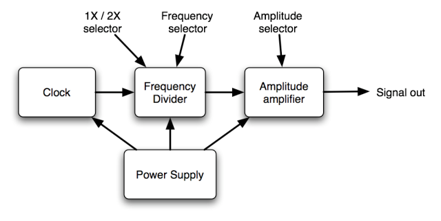
What does it do? The 4505 provides square wave output pulses at periods of 1uS, 10uS, .1mS, 1mS, 10mS, and 100mS. It also provides a feature to increase the periodicity of the signal by 2X and 5X. Lastly, output levels can be adjusted from 1mV to 100V in 10X steps. This functionality allows the technician to calibrate the scope's time base and vertical amplifier so it reads accurately. I put together a block diagram, below, which helps decompose the problem. We'll focus on the clock and frequency divider sections.
 Clock Circuit
The clock circuit in the IG-4505 circuit starts with a 4MHz crystal oscillator (see picture below, lower left, labeled 4MHz). This signal is then divided down to lower frequencies by TTL counters. Instead of a crystal, I happened to find some 4MHz ceramic resonators on my favorite electronics surplus site so I ordered a couple. They have about a ±0.5% precision with ±0.3% temperature drift, so about 12-32kHz error at 4MHz. That'd be terrible for calibrating a high precision frequency counter but it'll be fine for an analog oscilloscope. The error on a typical screen would be on the order of hundreths of an inch!
 The suggested drive circuitry on the resonator's datasheet is a little different than what's used in the Heathkit for the crystal, and requires a pair of CMOS inverters; that is, two gates from a 74HC04 IC. Apparently the crystal doesn't output enough current to drive anything but CMOS, since I tried a 74LS04 to no avail.
Upon wiring it up on the breadboard, this circuit produces a sort of ugly pseudo square wave, actually more like a capacitor charge/discharge waveform (or perhaps my oscilloscope isn't up to the task), but the signal is adequate to drive the counters. So that's the clock circuit.

 Frequency Divider
About the counters. Starting with 4MHz, we need to divide by 2 and again by 2 to arrive at a 1MHz signal. Then divide that signal by 2 for 2X. Divide that same signal by 5 for 5X. The Heathkit circuit uses 1/2 of a 7474 dual flip flop to do the initial ÷ 2 (2MHz). The flip flop is wired to output a pulse for every other clock pulse it receives.
 A 7490 Decade Counter is used to output pulses for ÷ 2 (1MHz) and ÷ 5 (400kHz). A switch selects the 1X/2X/5X signal. Then the other 1/2 of the 7474 is used for a final ÷ 2 to get the 1MHz, 0.5MHz, or 0.2MHz signal selected by the switch. Five 7490's are used to divide this signal by 10, 100, 1K, 10K, and 100K.
Since I couldn't easily find any 7474's or 7490's, I looked around for various counters and ran across the 74393 Dual Binary Counter and hte 74162 Decade Counter. The '393 has four output pins, one per bit of the 4-bit (nybble) count, call them Q0-Q3. The Q0 signal is 1/2 the frequency of the clock input and the Q1 signal is 1/4 the clock frequency.
In case you're not up on binary counters used as frequency dividers... Counting in binary (000, 001, 010, 011, 100, 101, 110, 111) the Q0 bit goes high every other clock pulse, so if we feed our 4MHz signal into the '393's clock pin, Q0 oscillates at 2MHz. Likewise, the Q1 output it goes high every 3rd and 4th clock pulse, half as often as Q0, and 1/4 as often as the clock pulse, or 1MHz in our case. I didn't want to bother with a 5X option so for now my plans are for a switch to select 1X or 2X.
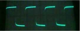
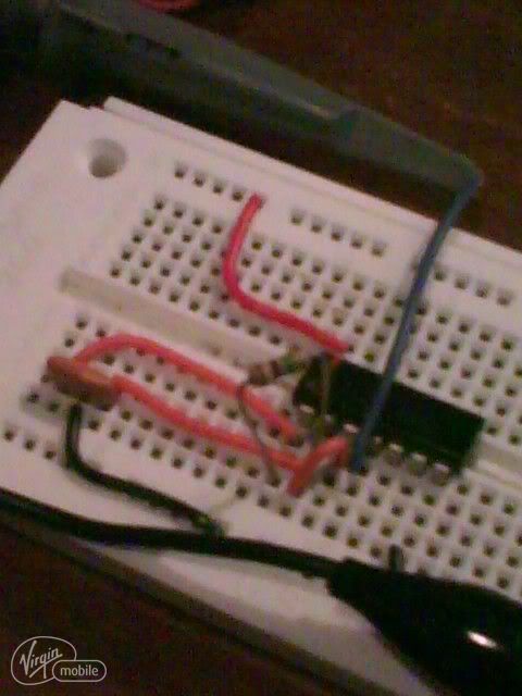
 On the breadboard, below left, I just hardwired the ÷ 4 (Q1) output. Initially I had problems getting the counter to work until I realized that the reset/clear/MR pin has to be wired low. Here's a scope trace showing the 1MHz pulsetrain on top and the original resonator/dual inverter output at the bottom.

 Finally, the 74LS162 I chose is a decade counter. You can configure it to do all sorts of things but what I wanted it to do was to count from 0 to 9, wrapping around to 0, and output a pulse every time the counter reaches 9 so as to generate a signal at 1/10th the clock frequency.
The chip provides a terminal counter (TC) aka ripple counter (RC0) pin, and there are a few pins that have to be set high to get the desired behavior, as described in the datasheet. ENT is Enable Terminal Counter, ENP is Enable Parallel, and the datasheet says to tie CLR to high through a resistor. The 1MHz Q1 output from the '393 is fed into the clock input of the '162.
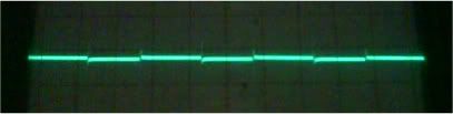
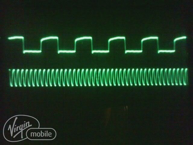
 Upon wiring this up on the breadboard (lower left), I was able to get pulses at a 100kHz frequency. The scope trace of the TC pin is shown at the top, the original 4MHz signal at the bottom. (By the way, I'm also finding my scope's timebase calibration is a little bit off).

 Since the 1MHz and ÷10 (100kHz) signals are covered, it's just a matter of sticking 4 more '162s into the circuit, just like the first, to add ÷100 (10kHz), ÷1K (1kHz), ÷10K (100Hz) and ÷100K (10Hz) signals. The circuit diagram for the complete set of '162s is below.
 The TC outputs of each '162 will feed to a rotary switch that'll select the period/frequency of the signal and pass it along to the amplitude amplifier, which I'll experiment with next.
But for now, the proof of concept I wanted to put together for the clock and frequency divider is done. And it actually worked! How cool is that?
Part 2: Amplitude
Part 3: Power Supply
Part 4: coming soon
EDIT: two years later I've revisited this circuit again and am in the process of finishing the build.
 |
| Heathkit IG-4505, photo from www.museudatecnologia.net.br |
I really would like an oscilloscope calibrator, like the Heathkit IG-4505, to tune up my 'scopes. Sure, I could spend the $30-60 on a used, pre-assembled specimen, even find an unassembled kit. In the meanwhile, I want to play around with the circuitry and possibly build my own from scratch. But how?
If you spend any time on Electro Tech Online, and if you're an old school digital logic kinda person like me, you quickly notice that the answer to all problems seems to be: "use a microcontroller." Ok, sure, a tiny little 8-pin DIP can easily solve a LOT of problems including this one and I may eventually build an MCU version of the calibrator.
Doing so misses out on they joy and thrill to be found in assembling a bunch of giant, antiquated PDIP logic ICs into something useful that requires no software and no PC (I can think of one blogger who would probably approve). Plus, a bunch of TTL ICs look cool on a breadboard. So today it's time to flash back to decades past when TTL ruled the world.
Rather than starting with a blank slate, an easier starting point is reverse engineering the Heathkit calibrator and emulating the circuit with similar ICs. I'll breadboard a prototype of the circuit to make sure this is going to work. The schematic can be found here. It comes in zip form, two pages.
Functionality
What does it do? The 4505 provides square wave output pulses at periods of 1uS, 10uS, .1mS, 1mS, 10mS, and 100mS. It also provides a feature to increase the periodicity of the signal by 2X and 5X. Lastly, output levels can be adjusted from 1mV to 100V in 10X steps. This functionality allows the technician to calibrate the scope's time base and vertical amplifier so it reads accurately. I put together a block diagram, below, which helps decompose the problem. We'll focus on the clock and frequency divider sections.
 Clock Circuit
The clock circuit in the IG-4505 circuit starts with a 4MHz crystal oscillator (see picture below, lower left, labeled 4MHz). This signal is then divided down to lower frequencies by TTL counters. Instead of a crystal, I happened to find some 4MHz ceramic resonators on my favorite electronics surplus site so I ordered a couple. They have about a ±0.5% precision with ±0.3% temperature drift, so about 12-32kHz error at 4MHz. That'd be terrible for calibrating a high precision frequency counter but it'll be fine for an analog oscilloscope. The error on a typical screen would be on the order of hundreths of an inch!
 The suggested drive circuitry on the resonator's datasheet is a little different than what's used in the Heathkit for the crystal, and requires a pair of CMOS inverters; that is, two gates from a 74HC04 IC. Apparently the crystal doesn't output enough current to drive anything but CMOS, since I tried a 74LS04 to no avail.
Upon wiring it up on the breadboard, this circuit produces a sort of ugly pseudo square wave, actually more like a capacitor charge/discharge waveform (or perhaps my oscilloscope isn't up to the task), but the signal is adequate to drive the counters. So that's the clock circuit.
About the counters. Starting with 4MHz, we need to divide by 2 and again by 2 to arrive at a 1MHz signal. Then divide that signal by 2 for 2X. Divide that same signal by 5 for 5X. The Heathkit circuit uses 1/2 of a 7474 dual flip flop to do the initial ÷ 2 (2MHz). The flip flop is wired to output a pulse for every other clock pulse it receives.
 A 7490 Decade Counter is used to output pulses for ÷ 2 (1MHz) and ÷ 5 (400kHz). A switch selects the 1X/2X/5X signal. Then the other 1/2 of the 7474 is used for a final ÷ 2 to get the 1MHz, 0.5MHz, or 0.2MHz signal selected by the switch. Five 7490's are used to divide this signal by 10, 100, 1K, 10K, and 100K.
Since I couldn't easily find any 7474's or 7490's, I looked around for various counters and ran across the 74393 Dual Binary Counter and hte 74162 Decade Counter. The '393 has four output pins, one per bit of the 4-bit (nybble) count, call them Q0-Q3. The Q0 signal is 1/2 the frequency of the clock input and the Q1 signal is 1/4 the clock frequency.
In case you're not up on binary counters used as frequency dividers... Counting in binary (000, 001, 010, 011, 100, 101, 110, 111) the Q0 bit goes high every other clock pulse, so if we feed our 4MHz signal into the '393's clock pin, Q0 oscillates at 2MHz. Likewise, the Q1 output it goes high every 3rd and 4th clock pulse, half as often as Q0, and 1/4 as often as the clock pulse, or 1MHz in our case. I didn't want to bother with a 5X option so for now my plans are for a switch to select 1X or 2X.
 On the breadboard, below left, I just hardwired the ÷ 4 (Q1) output. Initially I had problems getting the counter to work until I realized that the reset/clear/MR pin has to be wired low. Here's a scope trace showing the 1MHz pulsetrain on top and the original resonator/dual inverter output at the bottom.
The chip provides a terminal counter (TC) aka ripple counter (RC0) pin, and there are a few pins that have to be set high to get the desired behavior, as described in the datasheet. ENT is Enable Terminal Counter, ENP is Enable Parallel, and the datasheet says to tie CLR to high through a resistor. The 1MHz Q1 output from the '393 is fed into the clock input of the '162.
 Upon wiring this up on the breadboard (lower left), I was able to get pulses at a 100kHz frequency. The scope trace of the TC pin is shown at the top, the original 4MHz signal at the bottom. (By the way, I'm also finding my scope's timebase calibration is a little bit off).

 The TC outputs of each '162 will feed to a rotary switch that'll select the period/frequency of the signal and pass it along to the amplitude amplifier, which I'll experiment with next.
But for now, the proof of concept I wanted to put together for the clock and frequency divider is done. And it actually worked! How cool is that?
Part 2: Amplitude
Part 3: Power Supply
Part 4: coming soon
EDIT: two years later I've revisited this circuit again and am in the process of finishing the build.
Subscribe to:
Posts (Atom)