In Eagle, vias are square and overly large by default but you can change the default. All you have to do is create/edit eagle.scr in the scr directory of your Eagle installation. Enter the following lines:
Showing posts with label Eagle. Show all posts
Showing posts with label Eagle. Show all posts
Thursday, October 3, 2013

Thursday, September 12, 2013
Eagle: sudden clearance errors, isolation wrong?
You open up an Eagle board file only to find clearance errors when you run design rule check (DRC). Clearances that were working yesterday, and for the past hundred days on numerous boards, in fact.
Then you notice polygon isolation (clearance between polygon and trace) is too large. Pins that used to be connected to the polygon aren't. You can't manually reduce isolation. How do I fix this strange behavior?
Friday, December 7, 2012
Eagle: Improved Silk Generation
I finally fixed silk_gen.ulp. The new, improved silk_gen2.ulp (download) provides the following improvements...
I run the original silk_gen.ulp and afterwards, I run into several annoyances.
The script turns off the other layers. The bottom and top silk layers are the same color which is confusing.
It doesn't copy circles or polygons. I've hand-copied my logos way too many times.
Finally, it leaves the grid units set to "mil" regardless of what you had it set before.
After designing and re-designing a few dozen boards, I couldn't take it anymore. So I tweaked the ULP to fix the host of bugs and annoyances. Now I get this.

Ah, much better. My voices are happy for awhile longer.
Give it a try, share it, let me know if there are issues.
I'll likely post to the Eagle CAD website in the near future.
- Copies polygons and circles from source layers (tplace, tnames, etc.)
- Colors the bottom silk dark yellow (brown) so you can distinguish silk layers
- Displays top, bottom, unrouted, pads, and vias layers at the end instead of hiding them
- Preserves original unit setting instead of setting it to mil and leaving it
- Silk wire preserve the source wires width (bugfix)
- Correctly reproduce polygons without deleting the first wire (bugfix)
- Disabled silking of dimensions by default
- Selectable font (vector by default)
- Reproduces text layer, orientation angle and spin
 |
| Starting with a couple logos and polygons |
 |
| Well that's not very useful... |
It doesn't copy circles or polygons. I've hand-copied my logos way too many times.
Finally, it leaves the grid units set to "mil" regardless of what you had it set before.
After designing and re-designing a few dozen boards, I couldn't take it anymore. So I tweaked the ULP to fix the host of bugs and annoyances. Now I get this.

Ah, much better. My voices are happy for awhile longer.
I'll likely post to the Eagle CAD website in the near future.
Friday, September 28, 2012
Eagle CAD: Copying Between Schematics
Here's how to copy between schematics in Eagle CAD 6.1.0.
First of all, where is the CUT tool?! It's been replaced by the copy tool. You can now use that to copy between schematics.
First of all, where is the CUT tool?! It's been replaced by the copy tool. You can now use that to copy between schematics.
- Open one instance of Eagle CAD with your target schematic (TARGET)
- Open another instance of Eagle CAD with the source schematic you're copying from (SOURCE)
- SOURCE: In the source instance, use the Group tool
 to select what you want to copy
 - SOURCE: Click the copy tool

- SOURCE: Right-click on one of the parts and select Copy: Group from the contextual menu
- TARGET: click the Paste tool
 and paste your group wherever you want.
Friday, March 2, 2012
Eagle: Managing parts with BOM-EX

Here's Why
If you've designed and populated your own boards, you know that it's easy to spend lots of time finding the right parts.
A typical, simple board, like the LPC2101 breakout board I'm working on, has about a dozen unique parts. Big deal, you say.
It takes me about 5 minutes to find a suitable part using parametric search on DigiKey, Mouser, Newark, etc. A dozen parts means an hour of parts searching.
Wouldn't we all like to spend some of that time fixing your code or something? Besides, what about the next board you make? And the next? And the next? Having to search over and over for things is, well... sub-optimal.
There is an easier, faster way, my friends.
Friday, June 3, 2011
Diagonal components in Eagle
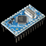 |
| Oooh! Diagonal chips are so cool! (Picture from Sparkfun) |
If only Eagle CAD could do that...
But it can!
You can position ANY component on your PCB to any arbitrary angle. And it's really easy. Here's how.
Let's look at this pesky bypass capacitor. There's no room between these traces for it. The board is jam packed. But hold on. If you mount the component diagonally it just might fit!

In the Board view, right click on the component in question and select Properties from the contextual menu.

In the properties dialog, simply edit the Angle field. For diagonal placement, enter 45°, 135°, 225°, or 315°. It doesn't matter as you can always rotate the component 90° at a time as before. Click ok, and then rotate the component as needed.
 |
| There, that's better. Diagonal fits! |
Voila, the little capacitor can now be squeezed in between these traces. Moving things around just a little bit, I was able to eliminate the DRC error (white box/line) and all was hunky dory.
Friday, September 3, 2010
Eagle Tips: Pour Regions
I draft all my circuits and board designs using Eagle from CadSoft. I've now drawn dozens of circuits and created several PCBs using this software. I picked up some tricks along the way.
Today's trick is: using ground pour polygons to simplify PCB routing
When designing PCBs, I find it easiest to hand route most of my designs to ensure the traces are exactly where I want them.
One way to simplify the routing task is to use a ground pour, or polygons, in Eagle. Basically what this means is filling in all the blank spots on the PCB with copper, and tying all the ground pins to this swath of copper.
Using a ground pour region also saves you time and etchant if you're doing your own PCBs at home, because there's less copper to remove.
Here's how.
Walk Through Example
I created a PCB, below, to interface Pokey with serial adapters; a BlueSMiRF Bluetooth modem and a Sparkfun FTDI serial to usb adapter.
Notice that there are large regions of the board colored blue, just like the other bottom traces. These regions are all part of the ground pour.
Let's rewind the clock and look at the serial board prior to laying it out. It looks like this. The components aren't yet placed on the board, outlined in white. No traces exist, only thin yellow lines representing the ratsnest.
Before you do anything else, create a polygon surrounding the board. Select the polygon tool (below left), draw a box around the outline of the board (below right). Make sure you're drawing the polygon on the Bottom (blue) layer.


Then right click the polygon outline, select Name from the contextual menu, and rename the polygon to GND which will connect it with the ground network in Eagle.
After you've created your ground pour, you can now move your components into place. If you click the ratsnest icon, the pour region will fill in and will connect any pin on the GND network to this pour region.
Isolate Pour and Traces
When doing my own PCBs at home, I find it helpful to put some space between the pour region and the traces. This is done with the Isolate parameter of the polygon. At home I find trace widths of about 0.024" to 0.032" are reasonable so this is the isolation setting I use.
Select the polygon, select properties, and choose 0.024" in the Isolation drop down menu.
NOTE: if a fabrication company is making your PCB, you may not be able to set isolation between the pour and the traces. Check with the vendor.
Use Orphans to Reduce Blank Spots
Sometimes there will be blank spots on the PCB that aren't contiguous with the ground pour, as in the example picture above. To minimize the blank areas on the board for home etching, you can have the ground pour create orphans, or islands of pour unconnected with anything else.
Kenneth, one of our readers, suggests we keep in mind that ungrounded blobs of copper can cause problems for high frequency signals. For home etching and low frequency it should be ok.
Select the polygon, select properties, and click the Orhpans checkbox. The default setting turns Orphans off.
Use Thermals for Easy Soldering
I've found it much easier to solder pins to the ground pour region when Thermals are used.
Instead of connecting the pin to a huge chunk of copper, which acts as a heat sink, and makes for blobby, cruddy solder joints, up to four thin traces connect the pin's pad to the larger region. The traces are easier to solder, I've found.
Select the polygon, select properties, and click the Thermals checkbox. This is the default.
Use Top Layer To Connect Grounds
Sometimes two ground pour regions are separated by a single trace, leaving the two regions disconnected. When you're etching single layer boards, you can still use top layer traces, implemented with wires, to fix the problem.
In the example below the vertical trace on the left that is marked by a white line is preventing the ground pour region from being contiguous. The unrouted line shows that the Ardweeny and bottom pin header ground aren't connected electrically.
You can convert part of a trace to reside on the top layer allowing the ground pour region to 'flow' underneath the jumper and connect the two regions.
Below, the vertical trace is converted to a top layer. The ground pour is now contiguous.
If your board will be two layer, no problem. If it's a one-layer board just use hookup or bus wire to implement the top layer.
Today's trick is: using ground pour polygons to simplify PCB routing
When designing PCBs, I find it easiest to hand route most of my designs to ensure the traces are exactly where I want them.
One way to simplify the routing task is to use a ground pour, or polygons, in Eagle. Basically what this means is filling in all the blank spots on the PCB with copper, and tying all the ground pins to this swath of copper.
Using a ground pour region also saves you time and etchant if you're doing your own PCBs at home, because there's less copper to remove.
Here's how.
Walk Through Example
I created a PCB, below, to interface Pokey with serial adapters; a BlueSMiRF Bluetooth modem and a Sparkfun FTDI serial to usb adapter.
 |
| Serial adapter with ground pour region |
Let's rewind the clock and look at the serial board prior to laying it out. It looks like this. The components aren't yet placed on the board, outlined in white. No traces exist, only thin yellow lines representing the ratsnest.
 |
| Components not yet laid out on the board to the right |


Then right click the polygon outline, select Name from the contextual menu, and rename the polygon to GND which will connect it with the ground network in Eagle.
 |
| Right click the polygon, select Name |
 |
| Enter GND as the polgyon's name |
 |
| After clicking ratsnest, notice ground pins are connected. |
When doing my own PCBs at home, I find it helpful to put some space between the pour region and the traces. This is done with the Isolate parameter of the polygon. At home I find trace widths of about 0.024" to 0.032" are reasonable so this is the isolation setting I use.
 |
| Without isolation between pour and traces |
 |
| With 0.024" isolation between traces and pour |
NOTE: if a fabrication company is making your PCB, you may not be able to set isolation between the pour and the traces. Check with the vendor.
Use Orphans to Reduce Blank Spots
Sometimes there will be blank spots on the PCB that aren't contiguous with the ground pour, as in the example picture above. To minimize the blank areas on the board for home etching, you can have the ground pour create orphans, or islands of pour unconnected with anything else.
Kenneth, one of our readers, suggests we keep in mind that ungrounded blobs of copper can cause problems for high frequency signals. For home etching and low frequency it should be ok.
Select the polygon, select properties, and click the Orhpans checkbox. The default setting turns Orphans off.
 |
| Orphans enabled; note fill in between the two traces |
Use Thermals for Easy Soldering
 |
| Thermal traces |
Instead of connecting the pin to a huge chunk of copper, which acts as a heat sink, and makes for blobby, cruddy solder joints, up to four thin traces connect the pin's pad to the larger region. The traces are easier to solder, I've found.
Select the polygon, select properties, and click the Thermals checkbox. This is the default.
Use Top Layer To Connect Grounds
Sometimes two ground pour regions are separated by a single trace, leaving the two regions disconnected. When you're etching single layer boards, you can still use top layer traces, implemented with wires, to fix the problem.
In the example below the vertical trace on the left that is marked by a white line is preventing the ground pour region from being contiguous. The unrouted line shows that the Ardweeny and bottom pin header ground aren't connected electrically.
 |
| The ground pour region is split. See the unrouted line? |
Below, the vertical trace is converted to a top layer. The ground pour is now contiguous.
 |
| The left vertical jumper fixes the ground pour split |
If your board will be two layer, no problem. If it's a one-layer board just use hookup or bus wire to implement the top layer.
Friday, August 6, 2010
Eagle Tips: Jumper Wires
I draft all my circuits and board designs using Eagle from CadSoft. Having drawn a couple dozen of circuits and PCB layouts using this software. I picked up some tricks along the way.
Today's trick is: using jumper wires when single sided routing won't work
For the home DIYer, single-sided PCB fabrication is well within reach. Double-sided, not so much. I find it easiest to hand route most of my designs to ensure the traces are exactly where I want them.
Occasionally, there is just no easy way to route every trace on the bottom. Using jumper wires on the top side of the board is a simple way to complete the single-sided design.
Here's how.
Walk Through Example
In upgrading Pokey my firefighting robot, I created a board to interface a Solarbotics Ardweeny (ATMega328P with a backpack board) to a GameBoy camera to detect flames.
I'd laid out the entire board but pin 12 and pin 26 on the ATMega328P still needed to be connected (see pink arrows below). There was no convenient way to do this on the bottom layer. Notice pin 12 has a trace going up to pin 8 of the top pin header, which is the camera interface.
Please ignore the vertical red trace on the left of the board. Its purpose will be discussed in another article.
The first step is to go ahead and draw a trace between pin 26 and the trace between pin 12 and the top pin header. See below. We're going to convert part of this new trace to a top layer jumper. Draw the trace so that there's a horizontal section separate from the rest of the trace.
Notice this new trace features a vertical section coming off pin 26, then a right angle and a long horizontal part. That horizontal section of the trace will become the jumper. If we didn't have the vertical part of the trace, the jumper would land on top of pin 26 and that just won't work.
Once you've drawn the trace and connected the pins, right click the horizontal section of the trace, and select Properties from the contextual menu.
Select the Top layer from the Layer pull down menu and click Ok.
The trace is now converted to the top layer and is colored red. Vias are added automatically. When you print your PCB design artwork for transfer, simply turn off visibility of the top layer. The resulting printout will include the vias for this trace, but not the top layer trace itself.
After etching your board, you can simply run a bus wire or hookup wire as a jumper between the two vias. This approach of using bus wire jumpers was common in a lot of 90's audio gear I've disassembled.
You can increase the size of the vias to something more normal like 0.039" or 0.031" diameter holes by right clicking each via, and choosing Properties from the contextual menu.
Then select the appropriate drill diameter from the Drill pull down menu for each.
Examples
Here are a couple more examples of my use of jumper wires on boards I've designed.
Today's trick is: using jumper wires when single sided routing won't work
For the home DIYer, single-sided PCB fabrication is well within reach. Double-sided, not so much. I find it easiest to hand route most of my designs to ensure the traces are exactly where I want them.
Occasionally, there is just no easy way to route every trace on the bottom. Using jumper wires on the top side of the board is a simple way to complete the single-sided design.
Here's how.
Walk Through Example
In upgrading Pokey my firefighting robot, I created a board to interface a Solarbotics Ardweeny (ATMega328P with a backpack board) to a GameBoy camera to detect flames.
I'd laid out the entire board but pin 12 and pin 26 on the ATMega328P still needed to be connected (see pink arrows below). There was no convenient way to do this on the bottom layer. Notice pin 12 has a trace going up to pin 8 of the top pin header, which is the camera interface.
Please ignore the vertical red trace on the left of the board. Its purpose will be discussed in another article.
 |
| How to connect pin 12 and 26? With a jumper... |
 |
| Draw trace. Ensure there's a horizontal section. |
Once you've drawn the trace and connected the pins, right click the horizontal section of the trace, and select Properties from the contextual menu.
 |
| Right click the trace and select Properties |
 |
| Select Top from the Layer menu to move the trace. |
 |
| Implement the top layer traces as jumper wires. |
You can increase the size of the vias to something more normal like 0.039" or 0.031" diameter holes by right clicking each via, and choosing Properties from the contextual menu.
 |
| Select Properties for each via |
 |
| Select the via's drill size from the pull down menu. |
Here are a couple more examples of my use of jumper wires on boards I've designed.
 |
| Serial board with jumper for handshaking |
 |
| Vertical jumper between V+ input and 555 timer IC's Vcc pin. |
Sunday, March 23, 2008
Circuit Design on Mac OS X
Circuit design is fine to do on paper for the simplest stuff but a CAD program is nice for everything else. I'd been using TinyCAD on my P3 400MHz, 128M desktop but am trying to move away from this glacially slow system, not to mention minimizing my exposure to Windows. :)
One good answer for Mac users is the free version of CadSoft Eagle running under the X11 windowing environment (follow the link to install X11). While it's not a seamless Aqua interface, it is actually a heck of a nice program once you get use to using it and it has an integrated PCB designer that works quite well. The user interface is a little bizzare, but with some practice I'm getting faster at drafting circuits. So far, the parts library seems to be pretty comprehensive, too.
If you want the app to show up in your Dock, you can write a shell script and use Platypus to create a wrapper application (may take several tries to figure it out) or try mine below which includes the shell script. Click on the link, save to disk, unzip, and copy the Eagle.app to /Applications. This app assumes the EAGLE-X11 folder is already installed in /Applications.
One good answer for Mac users is the free version of CadSoft Eagle running under the X11 windowing environment (follow the link to install X11). While it's not a seamless Aqua interface, it is actually a heck of a nice program once you get use to using it and it has an integrated PCB designer that works quite well. The user interface is a little bizzare, but with some practice I'm getting faster at drafting circuits. So far, the parts library seems to be pretty comprehensive, too.
If you want the app to show up in your Dock, you can write a shell script and use Platypus to create a wrapper application (may take several tries to figure it out) or try mine below which includes the shell script. Click on the link, save to disk, unzip, and copy the Eagle.app to /Applications. This app assumes the EAGLE-X11 folder is already installed in /Applications.

Subscribe to:
Posts (Atom)