Here's a review of free Linux Gerber file viewers.
PCB fabrication shops usually require Gerber files of your latest PCB design. Taking one last look can prevent mistakes, so you'll want to view the designs graphically with a Gerber file viewer.
Windows users have quite a few options which I've previously reviewed. For Linux users the choices are very limited but here's my review of the available options.
Showing posts with label PCB layout. Show all posts
Showing posts with label PCB layout. Show all posts
Wednesday, October 23, 2013

Friday, September 2, 2011
A Review of Free Windows Gerber File Viewers
When you send off your latest PCB design to a PCB fabrication shop you'll typically send Gerber files. You probably want to perform a final proof-read of your design, so you'll need a Gerber file viewer to view your files graphically. If you're cheap like me you want a free Gerber viewer. Here's a brief review of truly free Gerber file viewers for Windows.
Friday, June 3, 2011
Diagonal components in Eagle
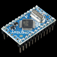 |
| Oooh! Diagonal chips are so cool! (Picture from Sparkfun) |
If only Eagle CAD could do that...
But it can!
You can position ANY component on your PCB to any arbitrary angle. And it's really easy. Here's how.
Let's look at this pesky bypass capacitor. There's no room between these traces for it. The board is jam packed. But hold on. If you mount the component diagonally it just might fit!

In the Board view, right click on the component in question and select Properties from the contextual menu.

In the properties dialog, simply edit the Angle field. For diagonal placement, enter 45°, 135°, 225°, or 315°. It doesn't matter as you can always rotate the component 90° at a time as before. Click ok, and then rotate the component as needed.
 |
| There, that's better. Diagonal fits! |
Voila, the little capacitor can now be squeezed in between these traces. Moving things around just a little bit, I was able to eliminate the DRC error (white box/line) and all was hunky dory.
Friday, September 3, 2010
Eagle Tips: Pour Regions
I draft all my circuits and board designs using Eagle from CadSoft. I've now drawn dozens of circuits and created several PCBs using this software. I picked up some tricks along the way.
Today's trick is: using ground pour polygons to simplify PCB routing
When designing PCBs, I find it easiest to hand route most of my designs to ensure the traces are exactly where I want them.
One way to simplify the routing task is to use a ground pour, or polygons, in Eagle. Basically what this means is filling in all the blank spots on the PCB with copper, and tying all the ground pins to this swath of copper.
Using a ground pour region also saves you time and etchant if you're doing your own PCBs at home, because there's less copper to remove.
Here's how.
Walk Through Example
I created a PCB, below, to interface Pokey with serial adapters; a BlueSMiRF Bluetooth modem and a Sparkfun FTDI serial to usb adapter.
Notice that there are large regions of the board colored blue, just like the other bottom traces. These regions are all part of the ground pour.
Let's rewind the clock and look at the serial board prior to laying it out. It looks like this. The components aren't yet placed on the board, outlined in white. No traces exist, only thin yellow lines representing the ratsnest.
Before you do anything else, create a polygon surrounding the board. Select the polygon tool (below left), draw a box around the outline of the board (below right). Make sure you're drawing the polygon on the Bottom (blue) layer.


Then right click the polygon outline, select Name from the contextual menu, and rename the polygon to GND which will connect it with the ground network in Eagle.
After you've created your ground pour, you can now move your components into place. If you click the ratsnest icon, the pour region will fill in and will connect any pin on the GND network to this pour region.
Isolate Pour and Traces
When doing my own PCBs at home, I find it helpful to put some space between the pour region and the traces. This is done with the Isolate parameter of the polygon. At home I find trace widths of about 0.024" to 0.032" are reasonable so this is the isolation setting I use.
Select the polygon, select properties, and choose 0.024" in the Isolation drop down menu.
NOTE: if a fabrication company is making your PCB, you may not be able to set isolation between the pour and the traces. Check with the vendor.
Use Orphans to Reduce Blank Spots
Sometimes there will be blank spots on the PCB that aren't contiguous with the ground pour, as in the example picture above. To minimize the blank areas on the board for home etching, you can have the ground pour create orphans, or islands of pour unconnected with anything else.
Kenneth, one of our readers, suggests we keep in mind that ungrounded blobs of copper can cause problems for high frequency signals. For home etching and low frequency it should be ok.
Select the polygon, select properties, and click the Orhpans checkbox. The default setting turns Orphans off.
Use Thermals for Easy Soldering
I've found it much easier to solder pins to the ground pour region when Thermals are used.
Instead of connecting the pin to a huge chunk of copper, which acts as a heat sink, and makes for blobby, cruddy solder joints, up to four thin traces connect the pin's pad to the larger region. The traces are easier to solder, I've found.
Select the polygon, select properties, and click the Thermals checkbox. This is the default.
Use Top Layer To Connect Grounds
Sometimes two ground pour regions are separated by a single trace, leaving the two regions disconnected. When you're etching single layer boards, you can still use top layer traces, implemented with wires, to fix the problem.
In the example below the vertical trace on the left that is marked by a white line is preventing the ground pour region from being contiguous. The unrouted line shows that the Ardweeny and bottom pin header ground aren't connected electrically.
You can convert part of a trace to reside on the top layer allowing the ground pour region to 'flow' underneath the jumper and connect the two regions.
Below, the vertical trace is converted to a top layer. The ground pour is now contiguous.
If your board will be two layer, no problem. If it's a one-layer board just use hookup or bus wire to implement the top layer.
Today's trick is: using ground pour polygons to simplify PCB routing
When designing PCBs, I find it easiest to hand route most of my designs to ensure the traces are exactly where I want them.
One way to simplify the routing task is to use a ground pour, or polygons, in Eagle. Basically what this means is filling in all the blank spots on the PCB with copper, and tying all the ground pins to this swath of copper.
Using a ground pour region also saves you time and etchant if you're doing your own PCBs at home, because there's less copper to remove.
Here's how.
Walk Through Example
I created a PCB, below, to interface Pokey with serial adapters; a BlueSMiRF Bluetooth modem and a Sparkfun FTDI serial to usb adapter.
 |
| Serial adapter with ground pour region |
Let's rewind the clock and look at the serial board prior to laying it out. It looks like this. The components aren't yet placed on the board, outlined in white. No traces exist, only thin yellow lines representing the ratsnest.
 |
| Components not yet laid out on the board to the right |


Then right click the polygon outline, select Name from the contextual menu, and rename the polygon to GND which will connect it with the ground network in Eagle.
 |
| Right click the polygon, select Name |
 |
| Enter GND as the polgyon's name |
 |
| After clicking ratsnest, notice ground pins are connected. |
When doing my own PCBs at home, I find it helpful to put some space between the pour region and the traces. This is done with the Isolate parameter of the polygon. At home I find trace widths of about 0.024" to 0.032" are reasonable so this is the isolation setting I use.
 |
| Without isolation between pour and traces |
 |
| With 0.024" isolation between traces and pour |
NOTE: if a fabrication company is making your PCB, you may not be able to set isolation between the pour and the traces. Check with the vendor.
Use Orphans to Reduce Blank Spots
Sometimes there will be blank spots on the PCB that aren't contiguous with the ground pour, as in the example picture above. To minimize the blank areas on the board for home etching, you can have the ground pour create orphans, or islands of pour unconnected with anything else.
Kenneth, one of our readers, suggests we keep in mind that ungrounded blobs of copper can cause problems for high frequency signals. For home etching and low frequency it should be ok.
Select the polygon, select properties, and click the Orhpans checkbox. The default setting turns Orphans off.
 |
| Orphans enabled; note fill in between the two traces |
Use Thermals for Easy Soldering
 |
| Thermal traces |
Instead of connecting the pin to a huge chunk of copper, which acts as a heat sink, and makes for blobby, cruddy solder joints, up to four thin traces connect the pin's pad to the larger region. The traces are easier to solder, I've found.
Select the polygon, select properties, and click the Thermals checkbox. This is the default.
Use Top Layer To Connect Grounds
Sometimes two ground pour regions are separated by a single trace, leaving the two regions disconnected. When you're etching single layer boards, you can still use top layer traces, implemented with wires, to fix the problem.
In the example below the vertical trace on the left that is marked by a white line is preventing the ground pour region from being contiguous. The unrouted line shows that the Ardweeny and bottom pin header ground aren't connected electrically.
 |
| The ground pour region is split. See the unrouted line? |
Below, the vertical trace is converted to a top layer. The ground pour is now contiguous.
 |
| The left vertical jumper fixes the ground pour split |
If your board will be two layer, no problem. If it's a one-layer board just use hookup or bus wire to implement the top layer.
Friday, August 6, 2010
Eagle Tips: Jumper Wires
I draft all my circuits and board designs using Eagle from CadSoft. Having drawn a couple dozen of circuits and PCB layouts using this software. I picked up some tricks along the way.
Today's trick is: using jumper wires when single sided routing won't work
For the home DIYer, single-sided PCB fabrication is well within reach. Double-sided, not so much. I find it easiest to hand route most of my designs to ensure the traces are exactly where I want them.
Occasionally, there is just no easy way to route every trace on the bottom. Using jumper wires on the top side of the board is a simple way to complete the single-sided design.
Here's how.
Walk Through Example
In upgrading Pokey my firefighting robot, I created a board to interface a Solarbotics Ardweeny (ATMega328P with a backpack board) to a GameBoy camera to detect flames.
I'd laid out the entire board but pin 12 and pin 26 on the ATMega328P still needed to be connected (see pink arrows below). There was no convenient way to do this on the bottom layer. Notice pin 12 has a trace going up to pin 8 of the top pin header, which is the camera interface.
Please ignore the vertical red trace on the left of the board. Its purpose will be discussed in another article.
The first step is to go ahead and draw a trace between pin 26 and the trace between pin 12 and the top pin header. See below. We're going to convert part of this new trace to a top layer jumper. Draw the trace so that there's a horizontal section separate from the rest of the trace.
Notice this new trace features a vertical section coming off pin 26, then a right angle and a long horizontal part. That horizontal section of the trace will become the jumper. If we didn't have the vertical part of the trace, the jumper would land on top of pin 26 and that just won't work.
Once you've drawn the trace and connected the pins, right click the horizontal section of the trace, and select Properties from the contextual menu.
Select the Top layer from the Layer pull down menu and click Ok.
The trace is now converted to the top layer and is colored red. Vias are added automatically. When you print your PCB design artwork for transfer, simply turn off visibility of the top layer. The resulting printout will include the vias for this trace, but not the top layer trace itself.
After etching your board, you can simply run a bus wire or hookup wire as a jumper between the two vias. This approach of using bus wire jumpers was common in a lot of 90's audio gear I've disassembled.
You can increase the size of the vias to something more normal like 0.039" or 0.031" diameter holes by right clicking each via, and choosing Properties from the contextual menu.
Then select the appropriate drill diameter from the Drill pull down menu for each.
Examples
Here are a couple more examples of my use of jumper wires on boards I've designed.
Today's trick is: using jumper wires when single sided routing won't work
For the home DIYer, single-sided PCB fabrication is well within reach. Double-sided, not so much. I find it easiest to hand route most of my designs to ensure the traces are exactly where I want them.
Occasionally, there is just no easy way to route every trace on the bottom. Using jumper wires on the top side of the board is a simple way to complete the single-sided design.
Here's how.
Walk Through Example
In upgrading Pokey my firefighting robot, I created a board to interface a Solarbotics Ardweeny (ATMega328P with a backpack board) to a GameBoy camera to detect flames.
I'd laid out the entire board but pin 12 and pin 26 on the ATMega328P still needed to be connected (see pink arrows below). There was no convenient way to do this on the bottom layer. Notice pin 12 has a trace going up to pin 8 of the top pin header, which is the camera interface.
Please ignore the vertical red trace on the left of the board. Its purpose will be discussed in another article.
 |
| How to connect pin 12 and 26? With a jumper... |
 |
| Draw trace. Ensure there's a horizontal section. |
Once you've drawn the trace and connected the pins, right click the horizontal section of the trace, and select Properties from the contextual menu.
 |
| Right click the trace and select Properties |
 |
| Select Top from the Layer menu to move the trace. |
 |
| Implement the top layer traces as jumper wires. |
You can increase the size of the vias to something more normal like 0.039" or 0.031" diameter holes by right clicking each via, and choosing Properties from the contextual menu.
 |
| Select Properties for each via |
 |
| Select the via's drill size from the pull down menu. |
Here are a couple more examples of my use of jumper wires on boards I've designed.
 |
| Serial board with jumper for handshaking |
 |
| Vertical jumper between V+ input and 555 timer IC's Vcc pin. |
Friday, August 28, 2009
Simple DIY PCB Etching
Want to fabricate printed circuit boards (PCB) at home, cheaply, quickly, and easily? So did I.
The tips on these sites worked for me but I have learned more. Read on....
Experimentation and perseverance help. It's ok if you goof up a few times; I did. Hang in there and you'll be a DIY pcb etching guru soon! Find out what works for you, and you're set.
Start with a small, simple circuit and stick to single sided traces! My first circuit was for a 12V/5V dual power supply circuit for another project. It uses only a handful of components.
The design layout fills a 2" square area, using up only a fraction of an already cheap (under $4) PCB blank from the local Radio Shack. In case the etching went poorly, I had enough PCB material to try it a few more times.
PCB Layout and Design
How did I do the printed circuit board layout in the first place? I like to use CadSsoft Eagle which does integrated schematic drawing and PCB layout. I can offer a some tips:

Can't figure out how to fit all the traces on one side? Cheat! Use jumper wires as in the board above and below. Many of the consumer electronics I've taken apart use bus wire. It's quick to install since there's no insulation to strip.

Several websites give tips on laser printing on magazine paper and transferring to the printed circuit board. Laser printing (and photocopying) uses melted plastic instead of ink. By applying heat heat, the plastic melts itself to the PCB, then the magazine paper can be soaked in water and rubbed off, leaving the laser print behind as a mask for the etching solution.
A few companies provide store bought solutions for transferring trace masks to the PCB but those are obviously more expensive than using scrap magazines. I haven't tried them yet.
Ricci Bitti's website gave the best advice. Printing on magazine paper was no problem and you can easily see the matte laserprint on the material.
Here are some additional tips:
Et voila, after six or more failed attempts, I finally got a good transfer!
 A few of the traces are a little blotchy, but none of the pads are. The fine detail turned out beautifully. Like you can see in the picture, the tiny printing and the crosshairs in the corner drill holes retained their detail.

I've since found better results when using traces no wider than 32 mil with good results at 24 and 16 mil. Smaller traces are unlikely to work well. You can repair any flaws in the transfer with a fine tip or ultra fine tip Sharpie permanent marker which conveniently resists etchant.
Etching
The common chemical of choice for DIY PCB etching is ferric chloride and that's what i use. You can get it from Radio Shack . Use suitable disposable gloves to keep the FeCl off your hands. They stain everything yellow. You don't want to look like a Simpsons character. Work in a well ventilated area.
To speed up pcb etching times, I now use a hot water bath. Put the FeCl in a small disposable tupperware tub. Put water in an electric skillet (I use my reflow skillet). Of course don't use it for food anymore! Put the tub in the water, and heat up the water to somewhat below the "warm" setting.
Boards usually etch in about 15-30 minutes. Don't let it go too long or it'll etch through the toner. So check it after 15 minutes and ever 5 minutes after that. I no longer use the FeCl-soaked sponge method. Too messy!
Once your pcb etching is complete, dip the board in water to rinse and neutralize the FeCl then wipe off the toner with acetone (spray carb cleaner) and a paper towel.
On my first fabricated board (below) the etching worked really well and even the smallest printing came out perfectly. There were a couple of small spots of toner that separated leaving tiny spots on a couple traces that were a little etched.


Pseudo Silk Screen
You can do your own "silk screen" printing on the top layer, too. But without real silk screen. Just use the toner transfer method to transfer printing onto the top of the board to show what components go where.
Update
After fabricating many printed circuit boards over the last few years since I first wrote this article, I've been etching more surface mount boards using 16 mil traces with 0805 and 0603 size SMD components, as well as SOIC, SSOP, SOT-223, SOT-23 and 0.6mm QFP packages! Not bad for DIY, eh?
Here's a couple examples that turned out very nicely. The ability to transfer such fine detail opens up a world of possibilities in board design. I used a Reflow Skillet to populate both boards. I've since started using my Weller station with fine tip along with fine SMD tweezers for the small passives.
Conclusion
With a little experimentation and perseverance in the face of multiple failures, I was able to reliably etch my own through hole and surface mount printed circuit boards. If you follow these tips, you'll soon be doing the same and a new world of hobby electronics will open itself up to you..
But hey if you got this far and still don't feel comfortable trying it, then give oshpark.com a try. I highly recommend them and use them all the time. Affordable and outstanding quality.
Next: Drilling
The tips on these sites worked for me but I have learned more. Read on....
Experimentation and perseverance help. It's ok if you goof up a few times; I did. Hang in there and you'll be a DIY pcb etching guru soon! Find out what works for you, and you're set.
Start with a small, simple circuit and stick to single sided traces! My first circuit was for a 12V/5V dual power supply circuit for another project. It uses only a handful of components.
The design layout fills a 2" square area, using up only a fraction of an already cheap (under $4) PCB blank from the local Radio Shack. In case the etching went poorly, I had enough PCB material to try it a few more times.
PCB Layout and Design
How did I do the printed circuit board layout in the first place? I like to use CadSsoft Eagle which does integrated schematic drawing and PCB layout. I can offer a some tips:
 Use wirepads (search for wirepad in the Eagle libraries) or pin headers for external interfaces not appearing in the schematic, like the transformer secondary wires, in this case.
- Use the DRC dialog and Restring tab to change the size of pads; bigger pads are better for manual drilling.
- Put all traces on the bottom layer so when you print the transfer you can uncheck "mirror"
- When you print the PCB transfer, hide all the layers you don't want to appear as copper traces, then print with the "black" checkbox option set (see picture to the right)
- For off-board components like rotary switches, create a custom package in the Eagle library comprised only of wire pads but using the correct schematic symbol.
- Include dimension lines in the transfer print but make them at least 16 mil.
- Create fill areas (pour regions) with Eagle, particularly for GND, instead of leaving lots of blank spaces on the PCB. Saves etchant and time etching. It also saves time laying out the board.


Example of using Eagle Fill Area (Polygon) for GND
Can't figure out how to fit all the traces on one side? Cheat! Use jumper wires as in the board above and below. Many of the consumer electronics I've taken apart use bus wire. It's quick to install since there's no insulation to strip.

Jumper a trace on the "top" of the board with pads.
- Add two pads where you want your jumpers.
- Change their name to match the net you're trying to jumper (e.g., VCC).
- Draw a trace between these pads on the "top" side of the board (red) to represent the wire
- Draw traces on the bottom side (blue) to the pads.
- When you print the PCB (see below) hide the top layer.
- Drill the holes, and run wire between these two pads
Several websites give tips on laser printing on magazine paper and transferring to the printed circuit board. Laser printing (and photocopying) uses melted plastic instead of ink. By applying heat heat, the plastic melts itself to the PCB, then the magazine paper can be soaked in water and rubbed off, leaving the laser print behind as a mask for the etching solution.
A few companies provide store bought solutions for transferring trace masks to the PCB but those are obviously more expensive than using scrap magazines. I haven't tried them yet.
Ricci Bitti's website gave the best advice. Printing on magazine paper was no problem and you can easily see the matte laserprint on the material.
 |
| Toner transfer, ready to iron onto the PCB |
Here are some additional tips:
- Cut down the magazine paper and tape it to scrap laser paper to prevent jams
- Use the "Wool" (1 below Cotton, 2 below Linen) setting on your iron
- Use green ScotchBrite pads for cleaning, abrading the PCB
- Clean the board with acetone (carb/choke cleaner)
- Apply moderate pressure, and slow circular movement on the iron for about 60 seconds.
Et voila, after six or more failed attempts, I finally got a good transfer!
 A few of the traces are a little blotchy, but none of the pads are. The fine detail turned out beautifully. Like you can see in the picture, the tiny printing and the crosshairs in the corner drill holes retained their detail.
I've since found better results when using traces no wider than 32 mil with good results at 24 and 16 mil. Smaller traces are unlikely to work well. You can repair any flaws in the transfer with a fine tip or ultra fine tip Sharpie permanent marker which conveniently resists etchant.
Etching
The common chemical of choice for DIY PCB etching is ferric chloride and that's what i use. You can get it from Radio Shack
. Use suitable disposable gloves to keep the FeCl off your hands. They stain everything yellow. You don't want to look like a Simpsons character. Work in a well ventilated area.To speed up pcb etching times, I now use a hot water bath. Put the FeCl in a small disposable tupperware tub. Put water in an electric skillet (I use my reflow skillet). Of course don't use it for food anymore! Put the tub in the water, and heat up the water to somewhat below the "warm" setting.
Boards usually etch in about 15-30 minutes. Don't let it go too long or it'll etch through the toner. So check it after 15 minutes and ever 5 minutes after that. I no longer use the FeCl-soaked sponge method. Too messy!
Once your pcb etching is complete, dip the board in water to rinse and neutralize the FeCl then wipe off the toner with acetone (spray carb cleaner) and a paper towel.
On my first fabricated board (below) the etching worked really well and even the smallest printing came out perfectly. There were a couple of small spots of toner that separated leaving tiny spots on a couple traces that were a little etched.


Pseudo Silk Screen
You can do your own "silk screen" printing on the top layer, too. But without real silk screen. Just use the toner transfer method to transfer printing onto the top of the board to show what components go where.
- In Eagle, hide all layers except tplace, dimensions, tname, tvalue, and tdocu
- Use the 'smash' function to enable moving and resizing the labels
- Add any other text you want (name, copyright, copyleft, whatever)
- When printing, select print in black and select the mirror image checkbox
- It's best to drill holes before you silkscreen; it gives you something to align to.
- Align the printed image to the board and holes.
- Toner transfer the image onto the blank side of the board.
 |
| Try to do a better job of aligning your "silkscreen" than I... |
After fabricating many printed circuit boards over the last few years since I first wrote this article, I've been etching more surface mount boards using 16 mil traces with 0805 and 0603 size SMD components, as well as SOIC, SSOP, SOT-223, SOT-23 and 0.6mm QFP packages! Not bad for DIY, eh?
Here's a couple examples that turned out very nicely. The ability to transfer such fine detail opens up a world of possibilities in board design. I used a Reflow Skillet to populate both boards. I've since started using my Weller station with fine tip along with fine SMD tweezers for the small passives.
 |
| 16 mil traces with 0603 SMD components. |
 |
| Board populated with 0603, TSSOP-8, etc |
With a little experimentation and perseverance in the face of multiple failures, I was able to reliably etch my own through hole and surface mount printed circuit boards. If you follow these tips, you'll soon be doing the same and a new world of hobby electronics will open itself up to you..
But hey if you got this far and still don't feel comfortable trying it, then give oshpark.com a try. I highly recommend them and use them all the time. Affordable and outstanding quality.
Next: Drilling
Subscribe to:
Posts (Atom)