Today's trick is: using ground pour polygons to simplify PCB routing
When designing PCBs, I find it easiest to hand route most of my designs to ensure the traces are exactly where I want them.
One way to simplify the routing task is to use a ground pour, or polygons, in Eagle. Basically what this means is filling in all the blank spots on the PCB with copper, and tying all the ground pins to this swath of copper.
Using a ground pour region also saves you time and etchant if you're doing your own PCBs at home, because there's less copper to remove.
Here's how.
Walk Through Example
I created a PCB, below, to interface Pokey with serial adapters; a BlueSMiRF Bluetooth modem and a Sparkfun FTDI serial to usb adapter.
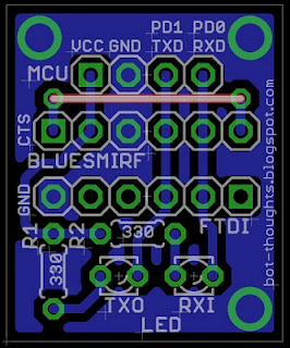 |
| Serial adapter with ground pour region |
Let's rewind the clock and look at the serial board prior to laying it out. It looks like this. The components aren't yet placed on the board, outlined in white. No traces exist, only thin yellow lines representing the ratsnest.
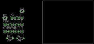 |
| Components not yet laid out on the board to the right |
Then right click the polygon outline, select Name from the contextual menu, and rename the polygon to GND which will connect it with the ground network in Eagle.
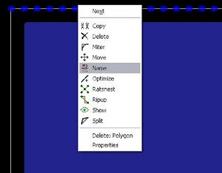 |
| Right click the polygon, select Name |
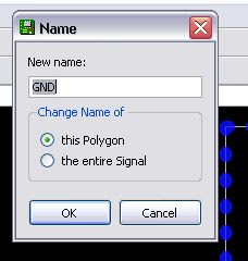 |
| Enter GND as the polgyon's name |
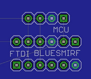 |
| After clicking ratsnest, notice ground pins are connected. |
When doing my own PCBs at home, I find it helpful to put some space between the pour region and the traces. This is done with the Isolate parameter of the polygon. At home I find trace widths of about 0.024" to 0.032" are reasonable so this is the isolation setting I use.
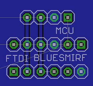 |
| Without isolation between pour and traces |
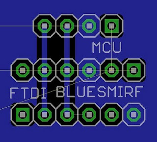 |
| With 0.024" isolation between traces and pour |
NOTE: if a fabrication company is making your PCB, you may not be able to set isolation between the pour and the traces. Check with the vendor.
Use Orphans to Reduce Blank Spots
Sometimes there will be blank spots on the PCB that aren't contiguous with the ground pour, as in the example picture above. To minimize the blank areas on the board for home etching, you can have the ground pour create orphans, or islands of pour unconnected with anything else.
Kenneth, one of our readers, suggests we keep in mind that ungrounded blobs of copper can cause problems for high frequency signals. For home etching and low frequency it should be ok.
Select the polygon, select properties, and click the Orhpans checkbox. The default setting turns Orphans off.
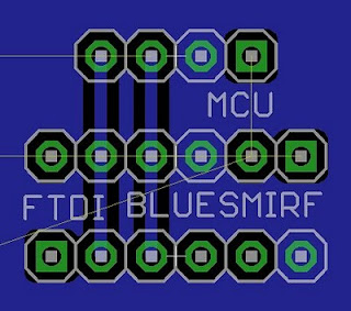 |
| Orphans enabled; note fill in between the two traces |
Use Thermals for Easy Soldering
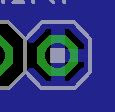 |
| Thermal traces |
Instead of connecting the pin to a huge chunk of copper, which acts as a heat sink, and makes for blobby, cruddy solder joints, up to four thin traces connect the pin's pad to the larger region. The traces are easier to solder, I've found.
Select the polygon, select properties, and click the Thermals checkbox. This is the default.
Use Top Layer To Connect Grounds
Sometimes two ground pour regions are separated by a single trace, leaving the two regions disconnected. When you're etching single layer boards, you can still use top layer traces, implemented with wires, to fix the problem.
In the example below the vertical trace on the left that is marked by a white line is preventing the ground pour region from being contiguous. The unrouted line shows that the Ardweeny and bottom pin header ground aren't connected electrically.
 |
| The ground pour region is split. See the unrouted line? |
Below, the vertical trace is converted to a top layer. The ground pour is now contiguous.
 |
| The left vertical jumper fixes the ground pour split |
If your board will be two layer, no problem. If it's a one-layer board just use hookup or bus wire to implement the top layer.


Thank you very much for your help.
ReplyDelete"In the example below, the vertical red trace is a jumper that allows the pour region to the left and the pour region that goes under the Ardweeny to connect up."
ReplyDeleteNo it doesn't.
@Anonymous: Can you offer more explanation for your thoughts here? I do see an issue with the diagram and will attempt to correct.
ReplyDelete[b]"Walk Through Example"[/b]
ReplyDeleteYou have made the integration of a copper pour with the ground plane simple. So simple it worked the first time I tried it!
YAY!
Thank you very much
for taking time to make this tutorial so simple. I will
read the rest of your EAGLE tips and become an EAGLE master! Thank you!
From an EMI/EMC perspective, orphaned copper on a PCB is not a good thing if it's not connected to ground. They can pick up signals and resonate. It's better to connect them to ground with vias or eliminate them altogether.
ReplyDeleteIf you are working on low-frequency stuff and just want to reduce the amount of copper you have to remove, then it's probably OK.
Kenneth, thanks for that tip!
DeleteFor home etching it's nice to reduce the amount of copper to remove. Otherwise I don't tend to use orphans.